Research Interests
Silicon Photonics for Biomedical Sensing
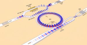
This research focuses on the design, simulation, and experimental characterization of silicon photonic sensors for biomedical applications. The research explores two key integrated photonic architectures: Mach–Zehnder interferometers (MZI) and Micro-Ring Resonators (MRR), which enable highly sensitive optical measurements through phase shifts, interference, and resonance changes.
Using numerical simulations, combined with experimental investigations of existing photonic devices, we aim to understand and optimize sensor performance, improve measurement accuracy, and develop robust methods for detecting small changes in refractive index and other relevant physical and biochemical parameters.
The research also investigates signal processing and machine learning techniques to enhance sensitivity, reduce noise, and compensate for environmental variations. Ultimately, this work aims to advance compact, sensitive, and potentially label-free photonic sensing technologies for biomedical monitoring and diagnostics, while creating opportunities for interdisciplinary collaboration.
Beyond biomedical sensing, silicon photonics offers promising opportunities for AI and quantum computing:
AI and Data Centers: Silicon photonics can enable high-bandwidth, energy-efficient optical interconnects, reducing communication power consumption and heat generation in AI data centers.
Quantum Computing: Photonic technologies offer opportunities for integrating optical components that enable the generation, manipulation, and measurement of quantum states.
Optical and Electrical Properties of Quantum Dots
Our research focuses on the optical and electrical behavior of quantum dots and their utilization in advanced engineering applications.
Quantum dots exhibit strong quantum confinement effects, leading to size-and composition-dependent optical absorption, emission, and charge transport properties.
The research combines optical spectroscopy and electrical characterization to study how material parameters and surface states affect device performance.
Applications include optoelectronics, sensing, biomedical imaging, and emerging quantum technologies.
This work emphasizes hands-on experimental methods and interdisciplinary approaches bridging electrical engineering, photonics, and materials science.
Optical Neuro-Monitoring for Early Detection of Epileptic Seizures (Aspire-Accelerated)
This research focuses on the development of optical sensing technologies for the early detection of epileptic seizures.
This work is based on the physiological principle that epileptic activity is associated with a rapid increase in cerebral metabolic demand,
leading to a pronounced and localized rise in brain oxygenation.
Using non-invasive optical measurement techniques inspired by pulse oximetry, the system detects fast oxygenation-related optical signatures
preceding or accompanying seizure onset. To achieve robust and reliable detection, the approach integrates sensor fusion methods,
combining optical signals with additional physiological inputs in order to discriminate epileptic events from confounding effects such as mechanical pressure or motion artifacts.
This project has been accepted into and is currently being incubated and accelerated by Aspire, Azrieli College’s innovation and entrepreneurship program.
The research bridges optics, biomedical engineering, and data-driven signal analysis, with the long-term goal of enabling wearable and continuous seizure monitoring solutions.
Representative Publications
1. Hechster, E. & Sarusi, G. (2017). Modeling the PbS quantum dots complex dielectric function by adjusting the E–k diagram critical points of bulk PbS. Journal of Applied Physics, 122(2), 024302.
https://doi.org/10.1063/1.4993123
2. Hechster, E. & Sarusi, G. (2015). Design and measurements of the absorption section of an up-conversion device based on PbSe quantum dots. Optical Materials, 50, 188–192.
https://doi.org/10.1016/j.optmat.2015.10.020
3. Hechster, E., Amgar, D., Arad-Vosk, N., Binyamin, T., Sa’ar, A., Etgar, L., & Sarusi, G. (2019).
Electrical and optical characterization of quantum dots PbS/TiO₂ based heterojunction as a SWIR detector and a proposed design of PbS/TiO₂-PeLED as a SWIR to visible up-conversion device.
Materials Research Express, 6, 066210.
https://doi.org/10.1088/2053-1591/ab0fb5
4. Arbel, M., Hechster, E. & Sarusi, G. (2016). Electrical conduction mechanisms in PbSe and PbS nanocrystals 3D matrix layer. AIP Advances, 6(2), 025314.
https://doi.org/10.1063/1.4942425
5. Hechster, E., Shapiro, A., Lifshitz, E. & Sarusi, G. (2016). Optical and electrical characterizations of a single-step ion-beam milling mesa device of chloride-passivated PbS colloidal quantum dot film. AIP Advances, 6, 075117.
https://doi.org/10.1063/1.4960013
6. Gabby Sarusi, Tzvi Templeman, Elad Hoxter, Nimrod Nissim, Vladimir Vitenberg, Nitzan Maman, Amir Tal, Assi Solodar, Guy Makov, Ibrahim Abdulhalim, Iris Visoly-Fisher, Yuval Golan,
“Architecture, development and implementation of a SWIR to visible integrated up-conversion imaging device,” Proc. SPIE 9884, Nanophotonics VI, 98840L (19 April 2016).
https://doi.org/10.1117/12.2231526